 Congratulations On Your Successful Submission
 Submission Failure
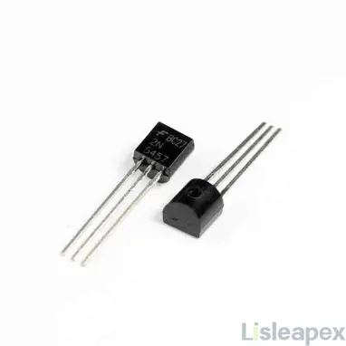
The 2N5457, a versatile N-Channel JFET transistor, stands as a cornerstone in electronic applications, excelling in signal amplification and low-level switching. With its compact TO-92 packaging, it offers high gain, low noise, and efficient low-power operation. Ideal for battery-operated devices, this transistor finds its place in audio equipment, amplifiers, and various small-signal applications. This comprehensive guide delves into its pinout, features, applications, and safe operation, providing valuable insights for engineers and enthusiasts.
What is 2N5457
The 2N5457 is a renowned TO-92 packaged JFET transistor designed for versatile applications in general-purpose switching and amplification. Some manufacturers also offer it in the SOT-23 package. Boasting high gain, low noise, and efficient low-power operation, this transistor finds utility in battery-operated devices. Tailored specifically for low-gain signal amplification, it excels in noise filtration, making it well-suited for various small-signal amplification tasks.
Functioning as an N-Channel JFET, the 2N5457 is engineered primarily for audio and switching applications. Its three terminals—drain (D), source (S), and gate (G)—comprise a voltage control device that operates without the need for bias current to regulate substantial currents across other terminals.
The 2N5457 belongs to the category of N-Channel Depletion Layer Junction Field Effect Transistors, widely applied in audio equipment for tasks such as amplification and tone modulation. Featuring a Drain-Source Voltage of 25 Vdc and a Drain-Gate Voltage of 25 Vdc, it is noteworthy for its reverse Gate-Source Voltage of -25V.
Where to Use & How to Use 2N5457
The 2N5457 is designed for signal amplification, making it suitable for various low-level signals, including audio. It can also function as a switch, handling a maximum load of 10mA in electronic circuits. Connect it appropriately for desired signal amplification or use it as a switch with attention to datasheet specifications for optimal performance.
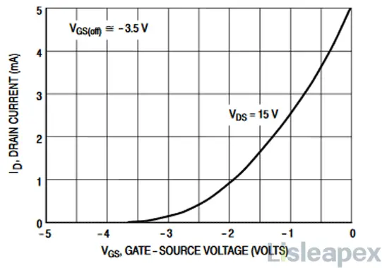
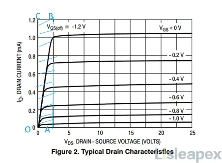
The graph presented below illustrates the common source transfer characteristic of the JFET, providing valuable insights into its operational behavior.
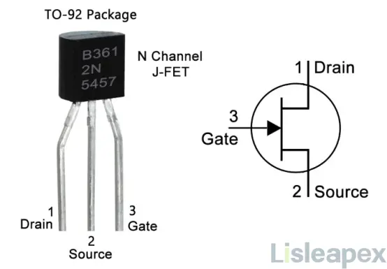
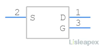
2N5457 Pinout
This diagram illustrates the pinout of the 2N5457 N-channel JFET. It has three pins – the left one is the drain, the middle one is the source, and the right one, labeled as 3, is the gate.
Pin Configuration
|
Number |
Pin Name |
Function |
|
1 |
Drain |
Drain pin |
|
2 |
Source |
Source pin |
|
3 |
Gate |
Gate pin |
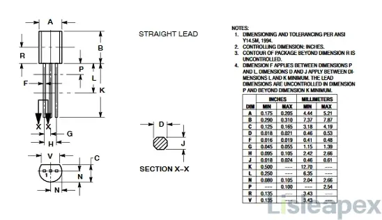
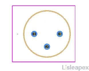
2D Model of 2N5257 N-channel JFET
The provided diagram illustrates the 2D representation of the 2N5257 N-channel Junction Field-Effect Transistor (JFET). It delineates the physical dimensions of the requisite components essential for the design of a printed circuit board (PCB) card.
2N5457 CAD Model
Symbol
Footprint
2N5457 Features and Specifications
Features
• N−Channel Configuration for Enhanced Gain
• Interchangeable Drain and Source
• Elevated AC Input Impedance
• Increased DC Input Resistance
• Reduced Transfer and Input Capacitance
• Minimal Cross−Modulation and Intermodulation Distortion
• Encapsulated in Plastic Package
• Pb−Free Packages Offered*
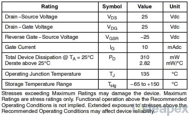
Specifications
|
Parameter |
Value |
|
Electrical Characteristics |
|
|
Drain-Source Voltage (Vds) |
25 Volts |
|
Drain-Gate Voltage (Vdg) |
25 Volts |
|
Gate-Source Voltage (Vds) |
-25 Volts |
|
Power Dissipation |
310 mW |
|
Gate Current |
10 mA |
|
Gate-Source Cutoff Voltage (Vds=15V, Id=10nA) |
-6.0 Volts |
|
Zero Gate Voltage Drain Current (15V, Vgs=0V) |
5.0 mA |
|
Package Information |
|
|
Package Type |
TO-92 |
|
Number of Pins |
3 |
|
Number of Terminations |
3 |
|
Height |
4.7 mm |
|
Width |
3.68 mm |
|
Weight |
201 mg |
|
Type and Operational Characteristics |
|
|
Type |
JFET - N - Channel - Depletion |
|
Segment |
General Purpose |
|
Drain to Source Voltage (VDS) |
25V |
|
Drain to Gate Voltage (VDG) |
25V |
|
Gate to Source Voltage (VGS) |
-25V |
|
Gate Current (IG) |
10 mA |
|
Gate-Source Cutoff Voltage - VGS (off) |
-6.0 Vdc (VDS = 15 Vdc, ID = 10 nAdc) |
|
Physical Dimensions |
|
|
Recommended Storage & Operating Temperature |
-55 to +150 degrees Celsius |
MAXIMUM RATINGS
2N5457 Application
The 2N5457 JFET is extensively utilized in analog switching and chopper applications, commonly recognized as a low-level amplifier or switching transistor. Its versatile applications are attributed to its low cross-modulation and intermodulation distortion characteristics, making it well-suited for a myriad of scenarios. Key applications include:
- Audio preamp circuits
- Amplification of low-level signals
- Sensor circuits
- Amplifier systems
- Audio amplifier stages
- IR detection (Infrared Detection)
- Small switching applications
- Audio modulation
- Tone control
- Noise generator
- Phase-shifting oscillators
- Current limiting systems
As a Switch
The 2N5457 functions as a switch when operating in the ohmic region, denoted by the highlighted section OABC in the typical drain characteristics diagram found in the 2N5457 datasheet. In this region, even at zero VGS, the transistor conducts current when VDS is positive and below the pinch-off voltage. Gradually increasing VGS widens the depletion layer, narrowing the conduction channel, and consequently, the channel resistance surges up to 100 times.
Utilizing the N-channel JFET's variable resistor characteristic in this region, designers leverage the increasing channel resistance to amplify the voltage drop, effectively employing the transistor as a switch.
As an Amplifier
The 2N5457 transistor, configured as an amplifier, employs a load resistor connected to the drain. The N-channel JFET's gate-source region is reverse-biased by connecting the gate (P-channel) to the negative end of the battery and the source (N-channel) to the positive side, denoted as VGG.
The source voltage (VS) for amplification is applied between the gate and source terminals, resulting in an overall input voltage composed of both VS and VGG. Prior to the application of the AC input, VGG maintains the gate-source reverse bias, causing a high depletion layer, a narrow conduction channel, and low drain current.
Upon introducing the AC input signal, with positive and negative cycles, the gate-source junction becomes forward-biased during the positive half-cycle. This reduction in the depletion layer increases current flow across the load resistor, leading to a heightened voltage drop and amplification during the positive AC input phase.
Switch Circuit and Chopper Circuit of 2N5457
In this section, we will explore two example circuits utilizing the 2N5457 N-channel JFET.
2N5457 Switch Circuit
The provided circuit diagram illustrates the utilization of the 2N5457 N-channel JFET as a switch.
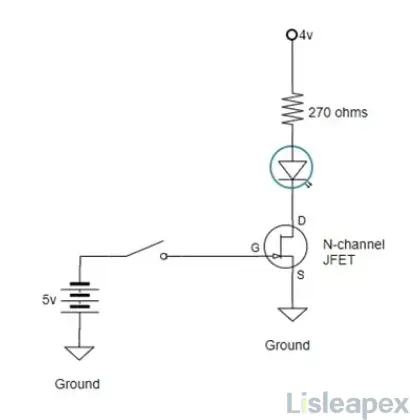
The N-channel JFET inherently operates in the "on" state at zero gate voltage, requiring no external biasing for current flow from drain to source. This signifies its saturation mode. When a voltage source is applied to the LED and there is no voltage at the JFET's gate terminal, the LED lights up. To deactivate the JFET and turn off the LED, a sufficient negative voltage must be applied to the gate terminal, inducing the JFET to enter the cut-off mode. Consequently, current ceases to flow from drain to source, causing the LED to lose its luminosity. The resistor is incorporated to limit the current through the LED, preventing potential damage.
2N5457 Chopper circuit
The diagram below illustrates the operational principle of a JFET as a chopper.
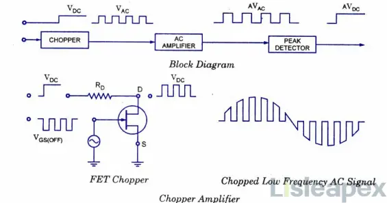
The occurrence of drift in circuits, stemming from temperature fluctuations and the coupling of direct and alternating currents in amplifiers, can be effectively addressed by employing choppers.
In this configuration, an input DC voltage undergoes modulation through a chopper, generating an alternating signal with an equivalent peak voltage as the initial DC input. Subsequently, the modulated signal is amplified using an AC amplifier, ensuring a drift-free operation. The amplified AC wave is subjected to peak detection to retrieve the amplified DC output signal.
To enable the JFET to function as a chopper, a square input signal is applied to the gate terminal, causing the JFET to alternate between saturation mode and cutoff mode.
Similar to the amplification of the input DC voltage without drift, an input AC voltage can also undergo amplification without introducing drift. A low AC input signal is introduced at the chopper, producing a modulated wave that is then amplified through an AC amplifier, effectively eliminating drift. The amplified wave is subsequently subjected to peak detection, restoring the original low-input AC signal initially applied to the chopper.
2N5457 - Interfacing Diagram
The image below illustrates the standard application of the N-Channel JFET 2N5457 as an amplifier. This circuit includes key components such as C1, a coupling capacitor, and C2, a DC blocking capacitor used to extract the output. RC represents the collector resistor, and modifying its value impacts the frequency response and controls the DC gain by regulating the collector current. R1 and R2 function as a voltage divider for biasing the JFET.
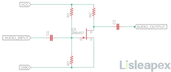
For a typical 12V operation, recommended values could be: R1 = 100k, R2 = 10k, RC = 10k, and C1, C2 can be 1uF ceramic capacitors. These values provide a basis for configuring the amplifier circuit to meet desired performance specifications.
How Does 2N5457 Safely Long Run in a Circuit
For optimal and safe long-term operation in a circuit with the 2N5457, it is advisable to adhere to the following guidelines:
- Current Limitation:
Ensure that the load does not exceed 10mA to prevent potential damage.
- Voltage Limitation:
Do not operate a load exceeding 25V through the transistor to stay within its specified voltage limits.
- Gate-Drain Voltage:
Avoid increasing the drain-to-gate voltage beyond 25V to prevent adverse effects.
- Reverse Gate-to-Source Voltage:
Exercise caution not to surpass -25V in reverse gate-to-source voltage, as this may compromise the transistor's performance.
- Temperature Range:
Operate and store the transistor within the temperature range of -55°C to +150°C to ensure reliable functionality and longevity.
2N5457 Advantages and Disadvantages
Advantages of 2N5457:
- Mechanical Efficiency: The 2N5457, known for its lightweight and compact size, is packaged in TO-92, featuring a robust shell for durable performance and effective insulation.
- High Impedance: Exhibiting high impedance, this JFET transistor is well-suited for applications requiring efficient signal processing.
- Low Power Consumption: With a characteristic of low power consumption, it proves to be energy-efficient, making it suitable for battery-operated devices.
- Compact Design: Designed in small form factors, the 2N5457 minimizes circuit space requirements, facilitating the creation of compact and space-efficient electronic circuits.
- Low Noise, High Gain: Characterized by low noise and high gain, it ensures effective signal amplification with minimal distortion, contributing to high-quality signal processing.
- Voltage-Sensitive Operation: Functioning as a voltage-sensitive device with high input impedance, the 2N5457 provides precise control over signals in various electronic applications.
- Preferred Input Stage: Often preferred over Bipolar Junction Transistors (BJTs) as the input stage in multi-stage amplifiers, showcasing its versatility in amplifier configurations.
Disadvantages of 2N5457:
- Temperature Sensitivity: Like many semiconductor devices, the performance of the 2N5457 can be sensitive to temperature variations.
- Limited Power Handling: The power dissipation capability of the 2N5457 is moderate, limiting its use in high-power applications.
- Voltage Sensitivity: The transistor's characteristics are sensitive to variations in voltage, and exceeding maximum ratings may lead to device failure.
- Single Polarity: Being an N-channel JFET, it operates primarily with negative gate-source voltage, which may limit its compatibility in certain circuit configurations.
- Availability: While it has been a widely used component, the availability of specific models may vary, and it's essential to check current market conditions.
2N5457 Alternative and Equivalent
Alternative Options to 2N5457:
2N5458:
- Similar to 2N5457, 2N5458 is an N-channel JFET transistor.
- It is often used for signal amplification in electronic circuits.
J107:
- J107 is an N-channel JFET with applications in amplification and switching circuits.
- Known for its high input impedance and low noise characteristics.
- BF246B is an N-channel JFET transistor used for low-power amplification.
- It is known for its high gain and low noise performance.
J309:
- J309 is another N-channel JFET transistor used for amplification and switching.
- It offers high input impedance and is suitable for low-power applications.
Replacement and Equivalent Transistors:
- 2N4339
- 2N4340
- J201
- 2N4338
- 2N4341
- 2N5458
- 2N5459
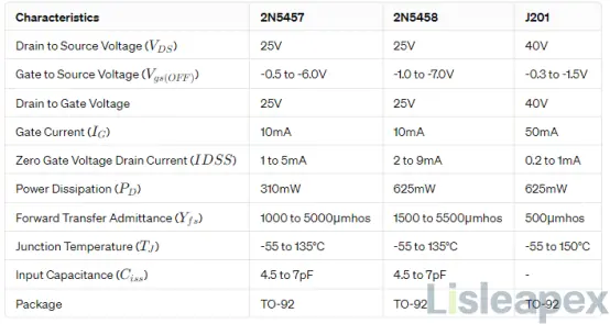
2N5457 vs 2N5458 vs J201:What are Differences
When comparing the electrical specifications of 2N5457, 2N5458, and J201, it's crucial for selecting the most suitable transistor for a given application. This table provides a comprehensive comparison of the electrical specifications for 2N5457, 2N5458, and J201.
Learn about N-channel JFET transistor
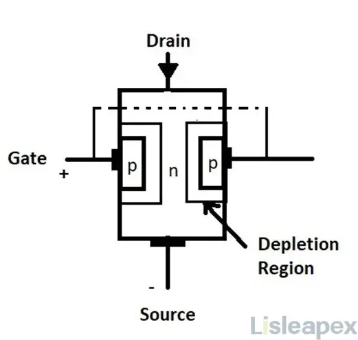
Working Principle of an N-channel JFET transistor
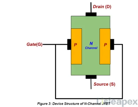
A Junction Field Effect Transistor (JFET) is comprised of three terminals: Gate, Drain, and Source, and can exist in two types: N-type and P-type. In the context of an N-type JFET, the gate terminal is connected to the p substrate, while the source and drain are linked to the n substrate. This configuration resembles a combination of two PN junctions, leading to the formation of depletion regions around the p substrates.
The application of input voltage occurs between the gate and the source terminals, while the output current is collected at the drain terminal. A notable feature of the JFET is its ability to conduct even in the absence of input supply. When the gate supply is zero and a positive voltage is applied between the drain and source, surpassing the transistor's pinch-off voltage, it initiates current conduction.
During a forward-biased condition of the input junction, the depletion layer diminishes, facilitating increased current flow in the drain. Conversely, in a reverse-biased condition, the opposite effect occurs. Armed with this foundational understanding, we can proceed to analyze the 2N5457 datasheet.
How to Choose a JFET transistor
To appropriately select a Junction Field Effect Transistor (JFET) for a specific application, follow these steps:
Choose JFET Type:
Identify the JFET type based on the application requirements. For example, for low-side power path applications, consider an N-Channel JFET like the 2N5457. For high-side switching, opt for a P-Channel JFET.
Calculate Maximum Voltage Ratings:
Calculate the maximum values for Drain-Source and Gate-Source voltages in the target application.
Select a JFET with breakdown voltages for Drain-Source and Gate-Source that exceed the calculated values.
For instance, the 2N5457 provides a 25V Drain-Source breakdown voltage and a -25V Gate-Source breakdown voltage.
Determine Maximum Drain Current:
Evaluate the maximum Drain Current required for the application.
Choose a JFET capable of handling a Drain current higher than the calculated requirement.
In the case of the 2N5457, it supports up to 0.005A of continuous Drain current (ID).
By following these steps, you ensure the selection of a suitable JFET that aligns with the voltage and current requirements of the targeted application.
Manufacturer
ON Semiconductor is a global semiconductor solutions provider headquartered in Phoenix, Arizona. Established in 1999, the company specializes in designing, manufacturing, and delivering a diverse range of semiconductor products. With a comprehensive portfolio covering power management, analog, mixed-signal, sensors, and connectivity solutions, ON Semiconductor serves industries such as automotive, industrial, communications, and consumer electronics.
Renowned for its expertise in power semiconductor technology, the company is committed to sustainable practices, innovation, and addressing societal challenges through semiconductor advancements. With a global presence and a mission to provide innovative solutions that shape the future of technology, ON Semiconductor is a key player in the semiconductor industry.
Datasheet PDF
Download 2N5457 datasheet PDF here>>
Conclusion
In conclusion, the 2N5457 N-Channel JFET emerges as a crucial component for diverse electronic endeavors. Its mechanical efficiency, high impedance, and low power consumption make it a preferred choice for amplification tasks. The provided pinout, specifications, and applications shed light on its capabilities, offering a roadmap for its utilization in different scenarios. Understanding its advantages, disadvantages, alternatives, and operational considerations ensures informed decision-making. As a fundamental building block in electronics, the 2N5457 continues to empower innovation in signal processing and low-power applications.
FAQ
-
What are some alternatives to the 2N5457?
Alternatives to the 2N5457 include other N-Channel JFETs with similar characteristics, such as the 2N5458 or 2N5459.
-
Can the 2N5457 be used in switching applications?
Yes, it can be used for switching applications where its voltage-controlled characteristics are advantageous.
-
Is the 2N5457 suitable for audio amplifier applications?
Yes, it is often used in audio amplifier circuits, especially in low-power and high-input-impedance designs.
-
How does the 2N5457 work?
The 2N5457 operates based on the voltage applied to the Gate terminal, which controls the flow of current between the Drain and Source terminals. It is a voltage-controlled device.
Stay updated with Lisleapex by signing up for the newsletter