 Congratulations On Your Successful Submission
 Submission Failure
Transistor technology has been advancing rapidly, with FinFETs emerging as a promising alternative to traditional MOSFETs. As semiconductor devices continue to shrink in size and increase in complexity, the demand for more efficient, high-performance transistors has grown exponentially.
In this comparative analysis, we delve into the differences between FinFET and MOSFET technologies, exploring their respective structures, operation principles, applications, and challenges. Understanding these distinctions is crucial for discerning which transistor technology is better suited for specific applications and for anticipating future developments in the semiconductor industry.
What is FinFET
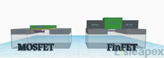
FinFET, short for Fin Field-Effect Transistor, is a type of multigate MOSFET (metal–oxide–semiconductor field-effect transistor) technology. It involves building transistors on a substrate where the gate surrounds the channel on multiple sides, forming a fin-like structure.
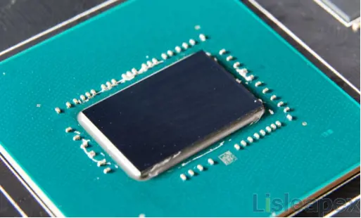
This design enhances performance with faster switching times and higher current density compared to traditional planar CMOS technology. FinFETs are essential in modern nanoelectronic semiconductor fabrication and have become prevalent in microchips at advanced process nodes like 14 nm, 10 nm, and 7 nm.
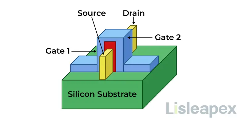
FinFET Diagram
FinFET, short for Fin Field-Effect Transistor, features a distinct 3D structure comprising a fin-like channel, surrounded by a gate. This architecture enables enhanced performance compared to traditional planar transistors. Now, let's delve into its key components:
- Fin: The central element of a FinFET, the fin is a vertical, 3D-shaped structure typically made of semiconductor material like silicon. It acts as the channel through which current flows.
- Gate: Surrounding the fin, the gate forms a 3D structure and is usually made of metal. Its primary function is to control the flow of electric current within the channel by modulating the conductance.
- Drain and Source: These terminals serve roles analogous to those in conventional MOSFETs. The source is where current enters the device, while the drain is where it exits. The gate regulates the flow of current between these terminals, facilitating the desired operation of the transistor.
FinFET Process Flow- How it Works?
The FinFET process flow encompasses several key steps to fabricate the three-dimensional transistor structure:
Lithography and Spacer-Based Patterning: Initially, the substrate undergoes lithography, involving the patterning of spacer-like structures on its surface. These spacers serve as guides for subsequent etching steps.
Formation of Vertical Trenches: Following lithography, an etching process is employed to carve vertical trenches into the substrate, creating the fin-like structures. These trenches define the fins' boundaries and dimensions.
Oxide Deposition and Fin Formation: The spaces between the vertical trenches are filled with oxide material through a deposition process. This step ensures the isolation and structural integrity of the fins. Subsequently, the top portion undergoes polishing to achieve a smooth surface finish.
Recess Etch: A recess etching step is carried out to precisely control the depth of the fins, ensuring uniformity and consistency across the substrate.
Gate Oxide Deposition and Gate Formation: Following fin formation, a layer of gate oxide is deposited on the surface. Then, the gate material is patterned and formed atop each fin structure. The gate controls the flow of current within the fin, with multiple gates typically implemented on each fin to optimize performance.
The FinFET process leverages these sequential steps to create a transistor structure where the channel is fully depleted and current control is achieved through gates positioned on multiple sides of the fin. This design enables improved performance, reduced power consumption, and enhanced scalability compared to traditional planar transistors.
FinFET Application
FinFET technology finds widespread application across various domains due to its numerous advantages over traditional planar transistors.
Microprocessors and CPUs: FinFET transistors are integral to the fabrication of high-performance microprocessors and central processing units (CPUs) used in computers, servers, and mobile devices. Their enhanced switching speed, lower power consumption, and improved scalability make them ideal for demanding computational tasks.
Graphics Processing Units (GPUs): FinFET technology is employed in the development of GPUs for gaming, artificial intelligence, data processing, and graphics-intensive applications. The advanced performance and energy efficiency of FinFETs contribute to improved graphics rendering, computational throughput, and overall system responsiveness.
System-on-Chip (SoC) Designs: FinFETs are crucial components in the fabrication of complex SoCs used in smartphones, tablets, IoT devices, and automotive electronics. Their compact size, reduced leakage current, and enhanced integration capabilities enable the creation of feature-rich, power-efficient, and high-performance semiconductor solutions.
Networking and Telecommunications: FinFET technology plays a vital role in the development of networking equipment, telecommunications infrastructure, and data center hardware. The increased transistor density, coupled with lower power consumption, enables the deployment of faster, more energy-efficient networking solutions capable of handling massive data volumes and supporting advanced communication protocols.
Artificial Intelligence (AI) and Machine Learning: FinFET transistors are utilized in AI accelerators, neural network processors, and machine learning algorithms to enable rapid data processing, pattern recognition, and predictive analytics. The superior performance characteristics of FinFETs contribute to the efficiency and scalability of AI-based applications in diverse fields such as healthcare, finance, and autonomous systems.
Automotive Electronics: FinFET technology is employed in automotive semiconductor solutions, including advanced driver assistance systems (ADAS), infotainment systems, and vehicle-to-everything (V2X) communication modules. The robustness, reliability, and performance efficiency of FinFETs make them well-suited for automotive applications demanding high computational power, real-time responsiveness, and stringent safety requirements.
Pros and Cons of FinFET
Pros:
- Enhanced Performance: FinFETs offer faster switching times and higher current density compared to traditional planar CMOS technology. This leads to improved speed and efficiency in electronic devices.
- Reduced Power Consumption: FinFETs consume less power due to their improved electrostatic control and reduced leakage currents. This results in longer battery life for mobile devices and lower energy consumption for other applications.
- Improved Scaling: FinFET technology allows for better scaling down to smaller process nodes, enabling the fabrication of more densely packed and higher-performing semiconductor chips.
- Better Control of Short-Channel Effects: The 3D structure of FinFETs helps mitigate short-channel effects, such as drain-induced barrier lowering and subthreshold slope degradation, which become more prominent at smaller transistor sizes.
- Higher Integration Density: FinFETs enable higher transistor density on a chip, leading to increased functionality and performance in complex integrated circuits.
Cons:
- Complex Fabrication Process: The fabrication process for FinFETs is more complex and costly compared to traditional planar transistors, requiring additional manufacturing steps and specialized equipment.
- Design Challenges: Designing circuits with FinFET technology requires adjustments to account for the unique characteristics of 3D transistor structures, such as gate pitch, fin width, and spacing, which can pose challenges for circuit designers.
- Process Variability: FinFET technology is more sensitive to process variations, leading to potential performance variations between individual transistors on a chip. This variability can impact yield and reliability in semiconductor manufacturing.
- Increased Design and Verification Complexity: The transition to FinFET technology necessitates changes to design and verification methodologies, as well as the adoption of new tools and techniques to ensure the reliability and functionality of integrated circuits.
- Higher Cost: The adoption of FinFET technology typically involves higher initial investment and manufacturing costs, which may be passed on to consumers in the form of higher-priced electronic devices.
What is MOSFET
The metal–oxide–semiconductor field-effect transistor (MOSFET) is a type of field-effect transistor (FET) primarily fabricated through controlled silicon oxidation. Featuring an insulated gate, the MOSFET's conductivity is regulated by the voltage applied to this gate. This property allows for efficient signal amplification or switching in electronic circuits.
The MOSFET's advantage lies in its minimal input current requirement to control the load current, distinguishing it from bipolar junction transistors (BJTs). It exists in two modes: enhancement, where gate voltage increases conductivity, and depletion, where it reduces conductivity. Despite the name, the "metal" gate can be composed of polysilicon, and various dielectric materials are utilized, making the MOSFET versatile in digital circuit applications, commonly found in memory chips and microprocessors due to its widespread use and scalability.
MOSFET Structure
The MOSFET structure consists of four terminals: Source (S), Drain (D), Gate (G), and body (B). However, the body terminal is often connected to the source, reducing the effective terminals to three. Charge carriers, either electrons or holes, traverse a channel whose width is modulated by the voltage applied to the Gate electrode, situated between the source and drain.
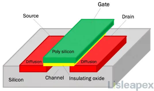
This modulation is facilitated by an insulating layer, typically metal oxide, separating the Gate from the channel. The MOSFET is synonymous with other terms such as metal-insulator-semiconductor field-effect transistor (MISFET) and insulated-gate field-effect transistor (IGFET).
2 Types of MOSFET
MOSFETs are categorized into different types based on their operation modes and doping configurations:
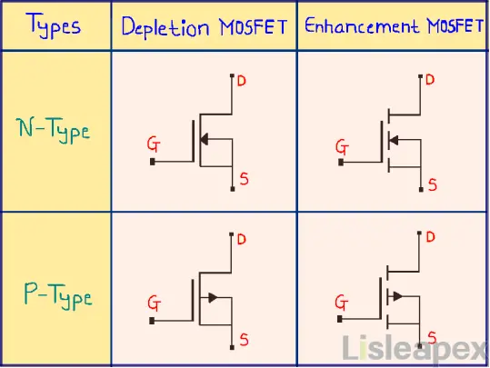
P-Channel MOSFET:
A P-Channel MOSFET utilizes positively charged holes as the majority carriers for current conduction. It consists of p-type drain and source regions and an n-type substrate. Applying a negative voltage to the gate relative to the source turns the transistor off, while a positive voltage turns it on. P-Channel MOSFETs find applications in power management circuits and CMOS integrated circuits.
N-Channel MOSFET:
An N-Channel MOSFET employs negatively charged electrons as the majority carriers for current conduction. It features n-type drain and source regions and a p-type substrate. Applying a positive voltage to the gate relative to the source turns the transistor off, while a negative voltage turns it on. N-Channel MOSFETs are commonly used in amplifiers, switching circuits, and digital logic circuits.
In both P-Channel and N-Channel MOSFETs, the gate voltage modulates the conductivity of the channel, either depleting it (Depletion Mode) or enhancing it (Enhancement Mode), thereby controlling the flow of current between the drain and source terminals. The specific doping configurations and operation modes determine the characteristics and applications of each type of MOSFET.
Working Principle of MOSFET
The operation of a MOSFET relies on the behavior of the MOS capacitor, which forms its essential component. Positioned between the source and drain terminals, the semiconductor surface beneath the oxide layer can transition from p-type to n-type in response to applied gate voltages.
Applying a positive gate voltage induces a repulsive force on holes beneath the oxide layer, causing them to move downward into the substrate. This action populates the depletion region with bound negative charges associated with acceptor atoms, facilitating electron flow and channel formation. Simultaneously, the positive voltage attracts electrons from the n+ source and drain regions into the channel.
When a voltage is subsequently applied across the drain and source, current flows freely through the channel, with the gate voltage regulating the movement of electrons. Conversely, applying a negative voltage results in the formation of a hole channel beneath the oxide layer.
MOSFET Application
MOSFETs find extensive applications across various fields due to their versatile characteristics and functionalities.
Power Electronics: MOSFETs are widely used in power electronics for switching applications, such as in DC-DC converters, AC-DC converters, motor control circuits, voltage regulators, and power inverters. Their high switching speed, low on-state resistance, and ability to handle high currents make them ideal for power management and control.
Amplification: MOSFETs are employed in amplifier circuits for audio amplification, RF amplification, and signal conditioning. They offer high input impedance, low output impedance, and low distortion, making them suitable for various audio and radio frequency applications.
Digital Integrated Circuits: MOSFETs are the fundamental building blocks of digital integrated circuits (ICs), including microprocessors, memory chips, and digital signal processors (DSPs). They serve as switching devices in logic gates, flip-flops, and other digital circuits, enabling the processing and storage of digital information in electronic devices.
Analog Integrated Circuits: MOSFETs are utilized in analog integrated circuits for voltage amplification, current amplification, and signal processing. They are essential components in operational amplifiers (op-amps), voltage regulators, filters, oscillators, and sensor interfaces, contributing to the functionality and performance of analog electronic systems.
Radio Frequency (RF) Applications: MOSFETs are employed in RF circuits for wireless communication systems, including cellular networks, Wi-Fi routers, Bluetooth devices, and radar systems. They are used as RF switches, power amplifiers, mixers, and oscillators, providing high-frequency performance and efficient signal transmission.
Pros and Cons of MOSFET
Pros of MOSFETs:
- High Efficiency: MOSFETs offer high efficiency in power conversion and amplification, making them suitable for a wide range of applications including power electronics and signal processing.
- Fast Switching Speed: MOSFETs have fast switching speeds, enabling rapid on-off transitions in electronic circuits, which is essential for high-frequency switching applications.
- Low Power Consumption: MOSFETs consume minimal power when in the off state, contributing to energy-efficient operation in battery-powered devices and reducing heat dissipation in electronic systems.
- Simple Drive Circuitry: MOSFETs require relatively simple drive circuitry, making them easy to integrate into electronic circuits and reducing design complexity.
- High Input Impedance: MOSFETs offer high input impedance, minimizing loading effects and allowing for easy interfacing with other electronic components.
Cons of MOSFETs:
- Leakage Current: MOSFETs exhibit leakage current even when they are turned off, leading to power losses and reduced efficiency, particularly at smaller process nodes.
- Gate Capacitance: MOSFETs have inherent gate capacitance, which can cause capacitive coupling effects and affect high-frequency performance in certain applications.
- Gate Drive Voltage: MOSFETs require a certain threshold voltage to turn on fully, which may necessitate higher drive voltages and additional circuitry in some cases.
- Temperature Sensitivity: MOSFET performance can be affected by temperature variations, leading to changes in threshold voltage and on-state resistance.
- Manufacturing Complexity: As transistor sizes shrink and process nodes advance, MOSFET manufacturing becomes increasingly complex, requiring sophisticated fabrication techniques and tighter process control to achieve desired performance characteristics.
FinFET vs MOSFET: What are Differences
FinFET and MOSFET present notable disparities across various aspects of their design, performance, and application. MOSFETs typically feature a planar structure, whereas FinFETs utilize a three-dimensional or "fin" structure. While MOSFETs regulate conductivity through voltage control, FinFETs modulate gate width via voltage adjustment.
Additionally, FinFETs demonstrate lower leakage current and improved power efficiency compared to MOSFETs. In terms of speed and performance, FinFETs boast faster switching speeds, while MOSFETs exhibit moderate performance. Furthermore, FinFETs offer reduced transistor capacitance and better scalability in smaller nodes, enhancing integration capability.
However, their manufacturing process is more complex and costly compared to MOSFETs. Despite these differences, both technologies find applications across a wide range of industries, with FinFETs showing potential for further development in the future.
|
Aspect |
FinFET |
MOSFET |
|
Integration |
Improved integration capability |
Limited integration capability |
|
Leakage Current |
Lower leakage current |
Relatively higher leakage current |
|
Manufacturing Process |
More complex manufacturing process |
Relatively simpler manufacturing process |
|
Gate Control |
Voltage-controlled gate width |
Voltage-controlled conductivity |
|
Power Efficiency |
Improved power efficiency |
Relatively lower power efficiency |
|
Structure |
Three-dimensional or "fin" structure |
Planar structure |
|
Cost |
Higher manufacturing cost |
Lower manufacturing cost |
|
Transistor Capacitance |
Reduced transistor capacitance |
Higher transistor capacitance |
|
Speed and Performance |
Faster switching speed |
Moderate speed |
|
Scalability |
Better scalability in smaller nodes |
Limited scalability in smaller nodes |
|
Future Trends |
Further potential for development |
Limited potential for future improvements |
|
Applications |
Similar range of applications as MOSFET |
Wide range of applications |
FinFET vs MOSFET: Which is better
Determining whether FinFET or MOSFET is better depends on the specific requirements of the application and the priorities of the design. Each technology has its own strengths and weaknesses, which make it more suitable for certain scenarios:
FinFETs typically offer better power efficiency, lower leakage current, faster switching speeds, reduced transistor capacitance, and improved scalability in smaller nodes compared to traditional MOSFETs. These advantages make FinFETs particularly well-suited for high-performance and low-power applications, such as mobile devices, high-speed processors, and energy-efficient electronics.
On the other hand, MOSFETs have been widely used and optimized over many years, offering simplicity in manufacturing, lower production costs, and well-established performance characteristics. MOSFETs may be preferred for applications where cost-effectiveness, reliability, and established performance metrics are critical, such as in certain industrial and automotive applications.
Ultimately, the choice between FinFET and MOSFET depends on factors such as power efficiency requirements, speed and performance demands, manufacturing considerations, cost constraints, and the specific needs of the application. Both technologies have their own advantages and are suitable for different use cases within the semiconductor industry.
FinFET vs MOSFET: Challenges
FinFET Challenges:
The adoption of FinFET technology presents several challenges in semiconductor manufacturing and design. The complex fabrication process for FinFETs requires additional manufacturing steps and advanced equipment, leading to higher production costs.
Moreover, managing process variability in FinFET technology is crucial to ensure consistent device performance and yield. Designing circuits with FinFETs also poses challenges due to the unique characteristics of 3D transistor structures, necessitating the development of new design methodologies and tools. Additionally, integrating FinFETs into existing semiconductor manufacturing processes may encounter compatibility issues, further complicating the transition from planar CMOS technology to FinFET technology.
MOSFET Challenges:
While MOSFET technology has been widely used, it faces challenges related to leakage current, scaling limitations, and heat dissipation. MOSFETs exhibit higher leakage current, especially at smaller process nodes, impacting power efficiency and battery life in electronic devices. Scaling MOSFETs to smaller dimensions encounters limitations such as short-channel effects and gate leakage, affecting transistor performance and reliability.
Moreover, as transistor sizes shrink and power densities increase, efficient heat dissipation becomes critical to prevent overheating and ensure device reliability. Managing performance trade-offs and addressing manufacturing complexities are essential for advancing MOSFET technology to meet the evolving demands of electronic systems.
Comparative Analysis of FinFETS and MOSFETS PDF
Download FinFETS and MOSFETS PDF here>>
Conclusion
In conclusion, the comparison between FinFETs and MOSFETs highlights the unique characteristics, advantages, and challenges of each transistor technology. While FinFETs offer enhanced performance, power efficiency, and scalability, they also come with increased manufacturing complexity and design challenges. On the other hand, MOSFETs provide simplicity, reliability, and established performance metrics, albeit with limitations such as higher leakage current and reduced scalability.
Ultimately, the choice between FinFET and MOSFET depends on the specific requirements of the application, balancing performance, cost, and manufacturing considerations. As semiconductor technology continues to evolve, further advancements in transistor design and fabrication are expected to drive innovation and shape the future of electronics.
FAQ
-
What are the disadvantages of FinFET?
Complex fabrication process: FinFETs require a more complex manufacturing process compared to traditional planar MOSFETs, which can increase production costs. Increased design complexity: Designing circuits with FinFETs can be more challenging due to their unique three-dimensional structure, requiring specialized design techniques and tools. Higher sensitivity to process variations: FinFET performance can be more sensitive to variations in manufacturing processes, leading to potential yield issues and performance variations across chips.
-
Why are FinFETs better than MOSFETs?
Improved electrostatic control: FinFETs offer better electrostatic control over the channel, resulting in reduced leakage current and improved energy efficiency. Enhanced scalability: FinFETs allow for continued scaling of transistor dimensions, enabling higher transistor density and performance improvements without significant increases in power consumption. Lower sub-threshold slope: FinFETs exhibit lower sub-threshold slope, leading to better transistor switching characteristics and improved overall circuit performance. Reduced short-channel effects: FinFETs mitigate short-channel effects compared to traditional MOSFETs, allowing for better performance and reliability in smaller transistor geometries.
-
What will replace FinFET?
Gate-All-Around (GAA) transistors, such as Nanosheet FETs, are being explored as potential replacements for FinFETs in future semiconductor technologies. GAA transistors offer further improvements in electrostatic control, scalability, and performance compared to FinFETs.
-
What is better than MOSFET?
Beyond FinFETs, emerging transistor technologies such as Nanosheet FETs (NSFETs), Tunnel FETs (TFETs), and Spintronic devices are being researched as potential candidates to surpass the performance of traditional MOSFETs. These technologies aim to address issues such as power consumption, leakage current, and scalability while improving overall transistor performance.
-
What is a major disadvantage of a Mosfet?
High sensitivity to temperature: MOSFETs can experience significant changes in threshold voltage and performance with variations in temperature, which can affect circuit operation and reliability, especially in high-temperature environments.
Stay updated with Lisleapex by signing up for the newsletter