 Congratulations On Your Successful Submission
 Submission Failure
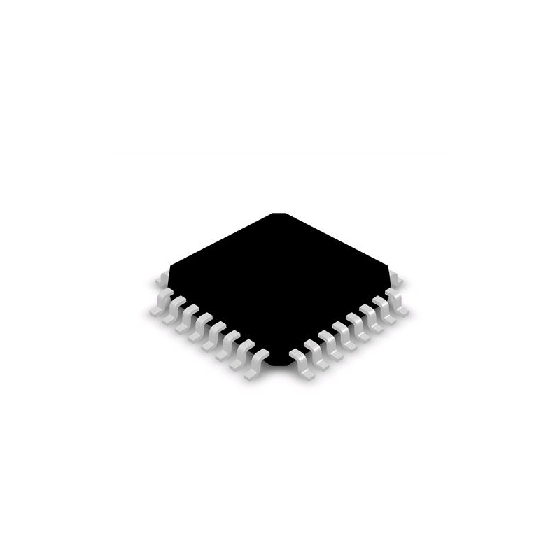
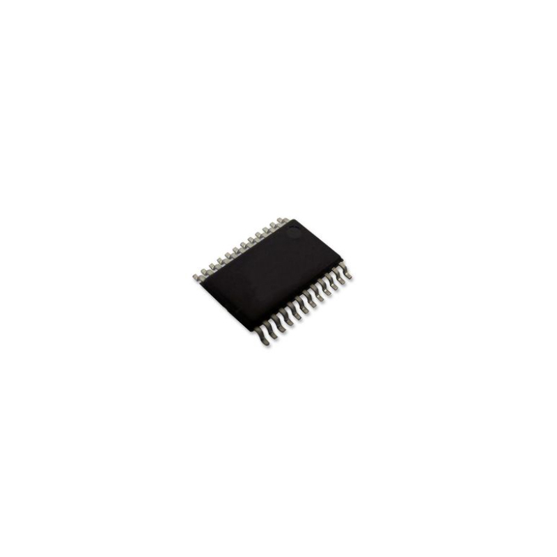
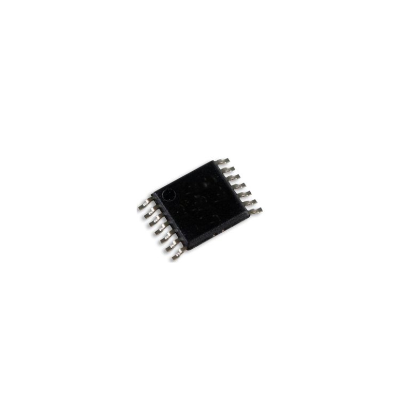
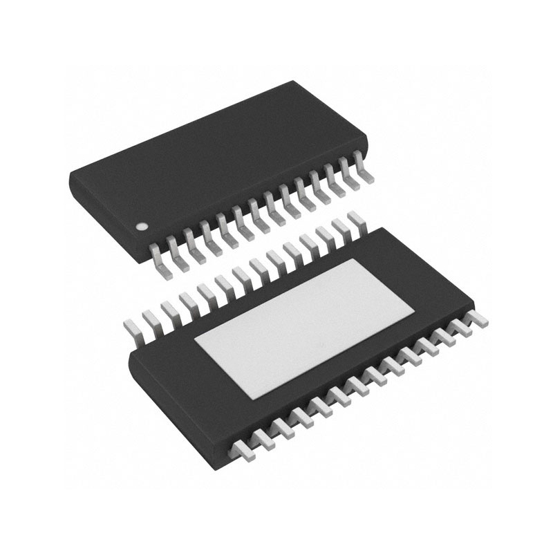
CDCVF2509APWR
Clock Generator 20MHz to 175MHz-IN 175MHz-OUT 24-Pin TSSOP T/RCDCVF2509APWR
Clock Generator 20MHz to 175MHz-IN 175MHz-OUT 24-Pin TSSOP T/R
-
Manufacturer Part # : CDCVF2509APWR
-
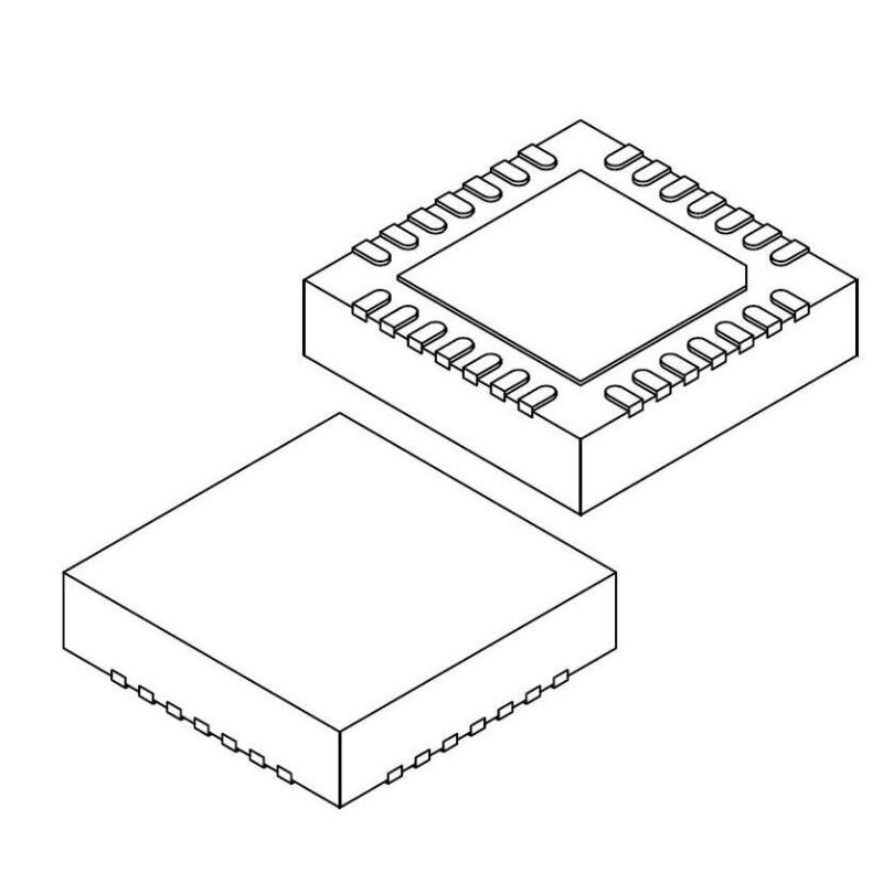
Package/Case: TSSOP
-
Part Status : ACTIVE
-
Brand: Texas Instruments
-
Product Categories : Clock buffers
-
RoHS:
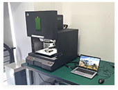
Quality Assurance
Quality Assurance
All parts procured from our supply chain network undergo a rigorous incoming inspection process. This meticulous inspection ensures that the parts received by our customers are authentic and meet the required standards. Additionally, we maintain detailed records of these inspections to ensure transparency and traceability throughout the supply chain.


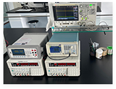
Certification
We have successfully obtained various certification standards and have established our own professional testing laboratory. This ensures that every product we supply to our customers meets the highest quality standards. We adhere to strict testing protocols to maintain the consistency and accuracy of our products. To ensure that our products are original and genuine, we also collaborate with reputable third-party testing facilities to conduct rigorous quality testing. Our commitment to quality extends to meeting industry, legal, regulatory, and ISO 9001:2015 requirements.
Shipping & Payment
Shipping & Payment
About Shipping
We generally ship orders within a few business days through reliable shipping carriers such as FedEx, SF, UPS, or DHL. We also have support for other shipping methods. If you would like to inquire about specific shipping details or costs, please don't hesitate to reach out to us.


About Payment
We accept various payment methods, including VISA, MasterCard, UnionPay, Western Union, PayPal, and other channels.
If you have a specific payment method in mind or would like to inquire about rates and other details, please feel free to contact us.

WireTransfer

Paypal

CreditCard

WesternUnion

MoneyGram
Service & Packaging
Service & Packaging
About After Sales Service
All Parts Extended Quality Guarantee
Initiate the application within 90 days from the shipment date.
Confirm the return or exchange with our staff.
Maintain the goods in their original condition as received.
Lastly, please note that the eligibility for return or exchange of goods is subject to an assessment of the actual condition of the returned items. We will evaluate the received goods before finalizing the return or exchange process. If you have any inquiries or require further assistance regarding returns or exchanges, please don't hesitate to contact us at [email protected]
About packaging
Regarding packaging, our products are carefully packed in anti-static bags to provide ESD anti-static protection. The outer packaging is durable with secure closure. We support various packaging methods such as Tape and Reel, Cut Tape, Tube, or Tray.

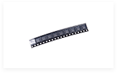
Example

Tape and Reel
Cut Tape
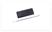
Tube or Tray
CDCVF2509APWR DataSheet
Pricing (USD)
| Quantity | Unit Price | Ext. Price |
|---|---|---|
| 1 | $9.805 | $9.80 |
| 200 | $3.795 | $759.00 |
| 500 | $3.661 | $1,830.50 |
| 1000 | $3.596 | $3,596.00 |
These prices are subiect to market fluctuations and quote submission is required.
Details
The CDCVF2509A is a high-performance, low-skew, low-jitter, phase-lock loop (PLL) clock driver. It uses a PLL to precisely align, in both frequency and phase, the feedback (FBOUT) output to the clock (CLK) input signal. It is specifically designed for use with synchronous DRAMs. The CDCVF2509A operates at a 3.3-V VCC. It also provides integrated series-damping resistors that make it ideal for driving point-to-point loads.
One bank of five outputs and one bank of four outputs provide nine low-skew, low-jitter copies of CLK. Output signal duty cycles are adjusted to 50%, independent of the duty cycle at CLK. Each bank of outputs is enabled or disabled separately via the control (1G and 2G) inputs. When the G inputs are high, the outputs switch in phase and frequency with CLK; when the G inputs are low, the outputs are disabled to the logic-low state. The device automatically goes into power-down mode when no input signal (< 1 MHz) is applied to CLK; the outputs go into a low state.
Unlike many products containing PLLs, the CDCVF2509A does not require external RC networks. The loop filter for the PLL is included on-chip, minimizing component count, board space, and cost.
For application information, see application reports High Speed Distribution Design Techniques for CDC509/516/2509/2510/2516 (SLMA003) and Using CDC2509A/2510A PLL with Spread Spectrum Clocking (SSC) (SCAA039).
The CDCVF2509A is characterized for operation from 0°C to 85°C.
Because it is based on PLL circuitry, the CDCVF2509A requires a stabilization time to achieve phase lock of the feedback signal to the reference signal. This stabilization time is required following power up and application of a fixed-frequency, fixed-phase signal at CLK, and following any changes to the PLL reference or feedback signals. The PLL can be bypassed by strapping AVCC to ground to use as a simple clock buffer.
Key Features
- Designed to Meet and Exceed PC133 SDRAM Registered DIMM Specification Rev. 1.1
- Spread Spectrum Clock Compatible
- Operating Frequency 20 MHz to 175 MHz
- Static Phase Error Distribution at 66 MHz to
166 MHz Is ±125 ps - Jitter (cyc - cyc) at 60 MHz to 175 MHz Is
Typ = 65 ps - Advanced Deep Submicron Process Results in More Than 40% Lower Power
Consumption Versus Current Generation PC133 Devices - Auto Frequency Detection to Disable Device (Power-Down Mode)
- Available in Plastic 24-Pin TSSOP
- Phase-Lock Loop Clock Distribution for Synchronous DRAM Applications
- Distributes One Clock Input to One Bank of Five and One Bank of Four Outputs
- Separate Output Enable for Each Output Bank
- External Feedback (FBIN) Terminal Is Used to Synchronize the Outputs to the Clock Input
- 25- On-Chip Series Damping Resistors
- No External RC Network Required
- Operates at 3.3 V
- APPLICATIONS
- DRAM Applications
- PLL Based Clock Distributors
- Non-PLL Clock Buffer
Specifications
The followings are basic parameters of the part selected concerning the characteristics of the part and categories it belongs to.
| Product Status | Obsolete | Programmable | Not Verified |
| Type | PLL Clock Driver | PLL | Yes with Bypass |
| Input | LVTTL | Output | LVTTL |
| Ratio - Input:Output | 2:10 | Differential - Input:Output | No/No |
| Frequency - Max | 175MHz | Divider/Multiplier | No/No |
| Voltage - Supply | 3V ~ 3.6V | Operating Temperature | 0°C ~ 85°C |
| Mounting Type | Surface Mount | Package / Case | TSSOP-24 |
| Supplier Device Package | 24-TSSOP | Base Product Number | CDCVF2509 |
| Manufacturer | Texas Instruments | Product Category | Clock Drivers & Distribution |
| RoHS | Details | Series | CDCVF2509A |
| Minimum Operating Temperature | 0 C | Maximum Operating Temperature | + 85 C |
| Mounting Style | SMD/SMT | Brand | Texas Instruments |
| Product | Clock Drivers | Product Type | Clock Drivers & Distribution |
| Factory Pack Quantity | 2000 | Subcategory | Clock & Timer ICs |
| Unit Weight | 0.003157 oz |
Recommend Parts
-
Clock Driver 10-OUT 2-IN 1:10 32-Pin LQFP Tray
Brand: Texas Instruments Package/Case: LQFP-32
7,150 In Stock
Cargo cycle: 3~7 Days
The minimum order is 1
-
Clock Buffer 4-output clock buffer for PCIe® Gen 1 to Gen 6 32-VQFN -40 to 105
Brand: Texas Instruments Package/Case: VQFN-32
8,558 In Stock
Cargo cycle: 3~7 Days
The minimum order is 1
-
CDCVF2310MPWREP
$12.194 Clock Fanout Buffer 10-OUT 1-IN 1:10 24-Pin TSSOP T/R
Brand: Texas Instruments Package/Case: TSSOP-24
8,864 In Stock
Cargo cycle: 3~7 Days
The minimum order is 1
-
CDCU877RHAR
$9.230 Zero Delay Buffer 10-Out Differential 40-Pin VQFN EP T/R
Brand: Texas Instruments Package/Case: VQFN-40
8,870 In Stock
Cargo cycle: 3~7 Days
The minimum order is 1
-
Clock Buffer Low Jitter2-Inp Sel 1:8 Univ-to-LVDS Bfr
Brand: Texas Instruments Package/Case: VQFN-28
6,814 In Stock
Cargo cycle: 3~7 Days
The minimum order is 1
-
Clock Buffer Lo Jitter 1:6 LVCMOS Fan-out Clock Bfr
Brand: Texas Instruments Package/Case: TSSOP-14
5,104 In Stock
Cargo cycle: 3~7 Days
The minimum order is 1
-
1.8 V 1.9 V Phase Lock Loop Clock Driver For Ddr2 SDRAM Applications 52 NFBGA
Brand: Texas Instruments Package/Case: NFBGA
6,802 In Stock
Cargo cycle: 3~7 Days
The minimum order is 1
-
Clock Divider/Fanout Buffer 4-OUT 1-IN 1:4 24-Pin VQFN EP T/R
Brand: Texas Instruments Package/Case: VQFN-24
6,909 In Stock
Cargo cycle: 3~7 Days
The minimum order is 1
-
CDC706PWR
$5.238 200-MHz, LVCMOS, custom-programmed 3-PLL clock synthesizer, multiplier & divider
Brand: Texas Instruments Package/Case: TSSOP
7,837 In Stock
Cargo cycle: 3~7 Days
The minimum order is 1
-
Clock Driver 10-OUT 1-IN 1:10 24-Pin SSOP T/R
Brand: Texas Instruments Package/Case: SSOP
5,686 In Stock
Cargo cycle: 3~7 Days
The minimum order is 1
-
Clock Synthesizer / Jitter Cleaner Hi Perf Lo Ph Noise Lo Skew Clock Synch
Brand: Texas Instruments Package/Case: BGA
6,589 In Stock
Cargo cycle: 3~7 Days
The minimum order is 1
-
CDCFR83ADBQ
$6.806 Clock Generator 533MHz-OUT 24-Pin SSOP Tube
Brand: Texas Instruments Package/Case: SSOP
5,461 In Stock
Cargo cycle: 3~7 Days
The minimum order is 1
-
Clock Generator 31.25MHz-IN 125MHz-OUT 24-Pin VQFN EP T/R
Brand: Texas Instruments Package/Case: VQFN EP
7,284 In Stock
Cargo cycle: 3~7 Days
The minimum order is 1
-
CDCDLP223PW
$2.220 Clock Generator 20MHz-IN 400MHz-OUT 20-Pin TSSOP Tube
Brand: Texas Instruments Package/Case: TSSOP
9,395 In Stock
Cargo cycle: 3~7 Days
The minimum order is 1
-
Clock Generator 27.35MHz to 38.33MHz-IN 1175MHz-OUT 24-Pin VQFN EP T/R
Brand: Texas Instruments Package/Case: VQFN-24
9,765 In Stock
Cargo cycle: 3~7 Days
The minimum order is 1
-
CDCVF855PWR
$4.269 Zero Delay Buffer 4-Out Differential 28-Pin TSSOP T/R
Brand: Texas Instruments Package/Case: TSSOP
6,270 In Stock
Cargo cycle: 3~7 Days
The minimum order is 1