 Congratulations On Your Successful Submission
 Submission Failure
In the realm of semiconductor technology, the PMOS (P-channel Metal-Oxide-Semiconductor) and NMOS (N-channel Metal-Oxide-Semiconductor) transistors stand as pillars of innovation, enabling the foundation of modern electronics. These two fundamental components, with their complementary operational principles, have revolutionized circuit design, paving the way for the development of integrated circuits and digital systems that power our technological world.

Understanding the structure, operation, and applications of PMOS and NMOS transistors is essential for engineers and enthusiasts alike, as they form the building blocks of countless electronic devices and systems.
PMOS vs NMOS: Symbol
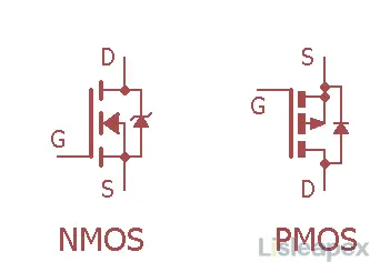
PMOS Symbol Description
The symbol for a PMOS (P-channel MOSFET) transistor also consists of three terminals: the source (S), the drain (D), and the gate (G).
Source (S): Represents the terminal where current exits the transistor. In a PMOS transistor, the source is connected to the highest voltage in the circuit, typically the power supply's positive terminal.
Drain (D): Represents the terminal where current enters the transistor. In a PMOS transistor, the drain is connected to the lowest voltage in the circuit, typically the ground or negative terminal of the power supply.
Gate (G): Controls the flow of current between the source and drain terminals. By applying a voltage between the gate and source (VGS), the conductivity of the transistor channel can be modulated.
NMOS Symbol Description
The symbol for an NMOS (N-channel MOSFET) transistor consists of three terminals: the source (S), the drain (D), and the gate (G).
Source (S): Represents the terminal where current enters the transistor. In an NMOS transistor, the source is connected to the lowest voltage in the circuit, typically the ground or negative terminal of the power supply.
Drain (D): Represents the terminal where current exits the transistor. In an NMOS transistor, the drain is connected to the highest voltage in the circuit, typically the power supply's positive terminal.
Gate (G): Controls the flow of current between the source and drain terminals. By applying a voltage between the gate and source (VGS), the conductivity of the transistor channel can be modulated.
PMOS vs NMOS: Definition
PMOS (P-channel Metal-Oxide-Semiconductor) and NMOS (N-channel Metal-Oxide-Semiconductor) transistors are fundamental components in electronics, especially in digital and analog circuits. They are both types of MOSFETs (Metal-Oxide-Semiconductor Field-Effect Transistors), which are crucial for building integrated circuits.
What is a PMOS Transistor
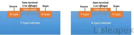
A PMOS transistor consists of a P-type semiconductor substrate with N-type source and drain regions. The gate, separated from the substrate by an insulating layer, controls the flow of current between the source and drain. In PMOS transistors, current flows when a negative voltage is applied to the gate, attracting positively charged holes from the source to the drain.
What is an NMOS Transistor
An NMOS transistor features an N-type semiconductor substrate with P-type source and drain regions. Similar to PMOS, the gate controls current flow between the source and drain. However, in NMOS transistors, current flows when a positive voltage is applied to the gate, drawing negatively charged electrons from the source to the drain.
In summary, PMOS and NMOS transistors are complementary in their operation. PMOS conducts when the gate voltage is low (or negative), while NMOS conducts when the gate voltage is high (or positive). This complementary behavior is utilized in designing efficient and low-power electronic circuits.
PMOS vs NMOS: Structure
PMOS (P-Channel Metal-Oxide-Semiconductor) and NMOS (N-Channel Metal-Oxide-Semiconductor) transistors are two fundamental components of modern electronic circuits, both utilizing the principle of Metal-Oxide-Semiconductor Field-Effect Transistors (MOSFETs). While they share similarities in structure and operational principles, they differ in doping types and configurations. PMOS transistors employ P-type semiconductor material for the source and drain regions, whereas NMOS transistors use N-type semiconductor material.
PMOS Transistor Structure
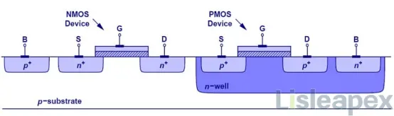
A PMOS transistor is fabricated on a semiconductor substrate typically composed of N-type silicon. P-type dopants, such as boron, are introduced into the substrate to form the source and drain regions, separated by a channel region within the N-type substrate. Above the channel region is the gate, isolated from the substrate by a thin layer of insulating material, typically silicon dioxide (SiO2). The gate is typically made of highly conductive materials such as polycrystalline silicon or metal.
When a voltage is applied between the source and drain terminals, a depletion region forms at the junction between the P-type source/drain regions and the N-type substrate. This depletion region acts as an insulating barrier, hindering current flow between the source and drain. However, upon applying a sufficient voltage to the gate terminal, an electric field is generated in the channel region, attracting positively charged holes from the P-type source and drain regions. As the gate voltage increases, more holes accumulate in the channel region, creating a conductive path between the source and drain, thereby enabling current flow.
NMOS Transistor Structure
The structure of an NMOS transistor is similar to that of a PMOS transistor, but with reversed doping types and configurations. In an NMOS transistor, the source and drain regions are formed by introducing N-type dopants, such as phosphorus or arsenic, into a P-type semiconductor substrate, typically silicon.
The N-type source and drain regions are separated by a channel region within the P-type substrate. Like the PMOS structure, the gate is positioned above the channel region and isolated from the substrate by a thin layer of insulating material, typically SiO2. The gate material is usually highly conductive, such as polycrystalline silicon or metal.
Upon applying a voltage between the source and drain terminals, a depletion region forms at the junction between the N-type source/drain regions and the P-type substrate. This depletion region acts as an insulating barrier, hindering current flow between the source and drain. However, when a sufficient voltage is applied to the gate terminal, an electric field is induced in the channel region, attracting negatively charged electrons from the N-type source and drain regions. As the gate voltage increases, more electrons accumulate in the channel region, establishing a conductive path between the source and drain, thus allowing current to flow.
PMOS vs NMOS: Working Principle
PMOS (P-Channel Metal-Oxide-Semiconductor) and NMOS (N-Channel Metal-Oxide-Semiconductor) transistors are two key components in electronic circuits, differing in their operating principles. PMOS transistors conduct current when a negative voltage is applied to the gate, while NMOS transistors conduct current when a positive voltage is applied to the gate.
How Does PMOS Work
PMOS transistors operate by controlling the conduction channel between the source and drain terminals via the gate voltage. When no voltage is applied to the gate, the transistor is in the default "on" state, allowing current flow between the source and drain. To turn off the PMOS transistor, a negative voltage is applied to the gate, repelling positively charged holes from the channel region, widening the depletion region, and blocking current flow.
How Does NMOS Work
NMOS transistors operate similarly but with reversed polarity. When no voltage is applied to the gate, the transistor is in the default "off" state, preventing current flow. To turn on the NMOS transistor, a positive voltage is applied to the gate, attracting negatively charged electrons to form a conductive channel between the source and drain.
PMOS vs NMOS: Application & Use
NMOS and PMOS transistors find extensive application in various electronic circuits, with popular uses including voltage amplifiers and switches. As "voltage to current" converters, both NMOS and PMOS transistors can be employed in amplifier circuits by incorporating resistive loads for output.
Three main amplifier configurations exist: common-source, common-drain, and common-gate, each with unique characteristics suited for different applications. Additionally, NMOS and PMOS transistors serve as effective switches due to their ability to provide large impedance when off and small impedance when on, making them valuable components in switched-mode power converters and digital logic circuits.
Application of PMOS
- CMOS Technology: PMOS transistors are integral components in complementary MOS (CMOS) technology, where they work in conjunction with NMOS transistors to form various digital logic circuits and integrated circuits.
- Voltage Level Shifters: PMOS transistors are commonly used in voltage level shifting circuits, where they help in converting high voltage signals to lower voltage levels, especially in applications like level shifters for I/O interfaces.
- Charge Pump Circuits: PMOS transistors are utilized in charge pump circuits to generate higher voltage levels from a lower voltage source, commonly used in applications like EEPROM programming and LCD biasing circuits.
- Overvoltage Protection: PMOS transistors are employed in overvoltage protection circuits to safeguard sensitive electronic components from damage by disconnecting the load from the power source when an overvoltage condition occurs.
Application of NMOS
- Digital Logic Circuits: NMOS transistors are fundamental components in digital logic circuits, where they are used in various configurations such as NAND gates, NOR gates, inverters, and transmission gates.
- Switched-Mode Power Supplies (SMPS): NMOS transistors are extensively used in SMPS applications, where they act as high-speed switches to regulate the flow of power between different components, ensuring efficient power conversion.
- Clock Drivers: NMOS transistors are employed in clock driver circuits to provide high-speed switching capabilities, crucial for maintaining synchronization in digital systems.
- Memory Arrays: NMOS transistors are used in memory arrays, such as dynamic random-access memory (DRAM), where they serve as access transistors for individual memory cells, enabling read and write operations.
Differences between NMOS and PMOS Transistors
NMOS (N-channel Metal-Oxide-Semiconductor) and PMOS (P-channel Metal-Oxide-Semiconductor) transistors are fundamental components in semiconductor technology, with NMOS utilizing electrons as majority charge carriers and PMOS utilizing holes. These transistors play vital roles in digital and analog circuits, offering high speed, low power consumption, and ease of integration. Complementary configurations of NMOS and PMOS transistors enable the development of complex integrated circuits, such as CMOS technology, which powers microprocessors, memory chips, and other digital logic circuits.
Differences between NMOS and PMOS Transistors:
|
Feature |
NMOS |
PMOS |
|
Majority Charge Carriers |
Electrons |
Holes |
|
Voltage Polarity for ON State |
Positive (Logic HIGH) |
Negative (Logic LOW) |
|
Channel Conduction Direction |
Source to Drain |
Drain to Source |
|
Substrate Biasing |
Bias to a voltage lower than Vss |
Bias to a voltage higher than Vdd |
|
Leakage Current |
Generally lower due to electron mobility |
Generally higher due to hole mobility |
|
On-Resistance |
Typically lower |
Typically higher |
|
Power Consumption |
Lower |
Higher |
|
Conduction Losses |
Lower |
Higher |
These differences stem from the intrinsic properties of electrons and holes in semiconductor materials, influencing transistor behavior and performance characteristics. NMOS and PMOS transistors complement each other in circuit design, with their unique features enabling efficient operation in various applications.
How to Choose between NMOS and PMOS Transistors
Choosing between NMOS (N-channel Metal-Oxide-Semiconductor) and PMOS (P-channel Metal-Oxide-Semiconductor) transistors depends on various factors related to the specific requirements of the circuit or system being designed. Here are some considerations to help you decide:
- Voltage Levels: NMOS transistors typically operate with positive gate voltages, making them suitable for circuits where positive voltage control is desired. On the other hand, PMOS transistors operate with negative gate voltages, making them suitable for circuits with negative voltage control.
- Speed and Performance: NMOS transistors generally have higher electron mobility and faster switching speeds compared to PMOS transistors. If high-speed operation is a priority, NMOS transistors may be preferred.
- Power Consumption: PMOS transistors typically have higher static power consumption due to their higher threshold voltages and lower electron mobility. If low power consumption is critical for your application, NMOS transistors may be a better choice.
- Circuit Topology: The choice between NMOS and PMOS transistors may also depend on the specific circuit topology and requirements. For example, in CMOS (Complementary Metal-Oxide-Semiconductor) logic circuits, both NMOS and PMOS transistors are used in complementary pairs to minimize static power consumption and improve noise immunity.
- Fabrication Technology: The availability of fabrication processes and technology may also influence the choice between NMOS and PMOS transistors. Some fabrication processes may be optimized for one type of transistor over the other, depending on factors such as cost, scalability, and performance.
- Voltage Level Shifting: PMOS transistors are commonly used in voltage level shifting circuits, where they help in converting high voltage signals to lower voltage levels, especially in applications like level shifters for I/O interfaces.
- Analog vs. Digital Circuits: Consider whether the circuit is primarily analog or digital in nature. NMOS transistors are often preferred in digital logic circuits due to their faster switching speeds, while PMOS transistors may be preferred in certain analog circuits due to their lower leakage current and potentially better matching characteristics.
Ultimately, the choice between NMOS and PMOS transistors requires careful consideration of the specific requirements and constraints of the circuit or system being designed, balancing factors such as speed, power consumption, voltage levels, and fabrication technology to achieve optimal performance and efficiency.
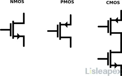
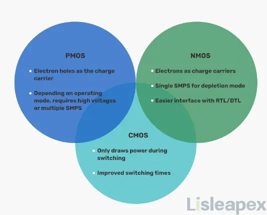
Differences between PMOS vs NMOS vs CMOS
PMOS Transistor:
PMOS transistors operate by controlling current flow between the source and drain terminals using a negative gate voltage. When the gate voltage is low, allowing positively charged holes to form a channel, the transistor conducts current. It is typically utilized in circuits where a negative voltage controls transistor behavior.
NMOS Transistor:
In contrast, NMOS transistors regulate current flow between the source and drain terminals with a positive gate voltage. When the gate voltage is high, attracting negatively charged electrons to form a channel, the transistor conducts current. It is commonly employed in circuits where a positive voltage controls transistor operation.
CMOS Technology:
CMOS technology combines both PMOS and NMOS transistors in a complementary configuration. This integration ensures that one type of transistor is on while the other is off, and vice versa, providing efficient operation. CMOS circuits offer low power consumption by eliminating a direct path between the supply voltage and ground in steady state. Moreover, they achieve high noise immunity by leveraging the complementary behavior of PMOS and NMOS transistors to cancel out electrical noise and interference effectively. CMOS technology is widely adopted in modern electronics for its efficient power usage and robust noise resistance, making it suitable for various applications ranging from digital logic circuits to microprocessors.
Here are main differences,
|
Aspect |
PMOS Transistor |
NMOS Transistor |
CMOS Technology |
|
Gate Voltage |
Negative |
Positive |
Complementary (Positive and Negative) |
|
Conduction |
Conducts current with low gate voltage |
Conducts current with high gate voltage |
Utilizes complementary behavior for efficient operation |
|
Typical Usage |
Circuits with negative voltage control |
Circuits with positive voltage control |
Widely used in modern electronics for various applications |
|
Power Consumption |
Relatively higher due to continuous hole flow |
Relatively lower due to electron flow |
Low due to complementary arrangement, minimal current flow in steady state |
|
Noise Immunity |
Susceptible to noise due to continuous hole flow |
More resistant to noise due to electron flow |
High, noise effects canceled by complementary behavior |
Challenges in PMOS and NMOS Transistor
Short-channel effect: As transistor dimensions shrink, the gate control over the channel weakens, leading to increased leakage current and reduced performance.
Gate leakage: Decreasing gate oxide thickness results in gate leakage, where electrons tunnel through the insulating layer, causing increased leakage current and power dissipation.
Hot carrier effects: High electric fields within the transistor can cause electrons to gain energy and become trapped in the gate oxide or damage the transistor structure, leading to performance degradation and reliability issues.
Subthreshold leakage: Subthreshold leakage occurs when the gate voltage is below the threshold voltage, resulting in a small amount of current flow between the source and drain even when the transistor is supposed to be off.
Bias temperature instability (BTI): Constant voltage stress at elevated temperatures can cause interface traps and oxide charges, leading to a shift in threshold voltage and reduction in drain current, affecting transistor performance over time.
Electromigration: Transport of metal ions due to high-density electric current flow can lead to voids and hillocks in metal interconnects, causing increased resistance, open circuits, or short circuits over time.
Conclusion
In conclusion, the PMOS and NMOS transistors represent not only technological achievements but also symbols of ingenuity and progress in the field of semiconductor engineering. As we continue to push the boundaries of miniaturization and efficiency, these transistors will remain at the forefront of innovation, driving advancements in areas such as computing, telecommunications, and renewable energy.
With their complementary characteristics and versatile applications, PMOS and NMOS transistors will continue to shape the landscape of electronics, inspiring generations of engineers to push the limits of what is possible in the realm of semiconductor technology.
FAQ
-
What Factors Influence the Choice Between PMOS and NMOS Transistors in Circuit Design?
The choice between PMOS and NMOS transistors depends on various factors, including power consumption requirements, speed considerations, circuit topology, voltage levels, and fabrication technology. Designers evaluate these factors to select the most suitable transistor type for their specific application.
-
How do PMOS and NMOS Transistors Complement Each Other in CMOS Logic?
In CMOS logic circuits, PMOS and NMOS transistors are combined to form complementary pairs, where one transistor is used to pull the output high (PMOS) and the other to pull it low (NMOS). This arrangement minimizes static power consumption and improves noise immunity in digital circuits.
-
What are the Applications of PMOS and NMOS Transistors?
PMOS and NMOS transistors are used in various applications, including digital logic circuits, analog circuits, power management circuits, and voltage level shifting circuits. PMOS transistors are often used in pull-up networks, while NMOS transistors are used in pull-down networks in CMOS logic.
-
What are the Differences in Electrical Characteristics Between PMOS and NMOS Transistors?
PMOS transistors typically have lower electron mobility and higher threshold voltages compared to NMOS transistors. As a result, PMOS transistors have slower switching speeds and higher static power consumption. However, PMOS transistors are advantageous in certain circuit configurations and power supply designs.
-
Which Transistor Type is More Commonly Used in CMOS Technology?
NMOS transistors were traditionally more commonly used in CMOS (Complementary Metal-Oxide-Semiconductor) technology due to their higher electron mobility and faster switching speeds. However, modern CMOS circuits typically use both PMOS and NMOS transistors to take advantage of their complementary characteristics.
Stay updated with Lisleapex by signing up for the newsletter