 Congratulations On Your Successful Submission
 Submission Failure
Hybrid integrated circuits (HICs) represent a pivotal advancement in electronic circuitry, blending the precision of semiconductor integration with the versatility of thin or thick film technology. These circuits, comprised of individual semiconductor devices and passive components, offer a unique solution for applications demanding specialized components that cannot be integrated into a single monolithic chip.
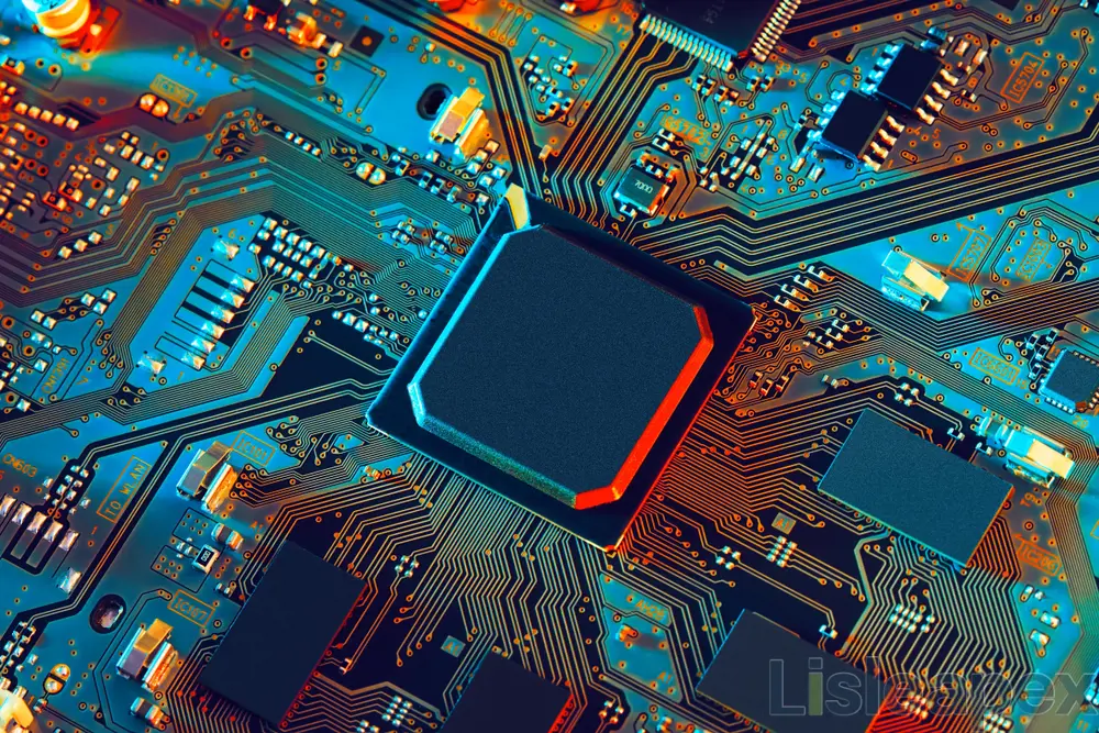
From telecommunications to automotive systems, HICs have played a crucial role in enabling high-precision, high-frequency, and high-power electronic systems. This article delves into the definition, development history, applications, key features, examples, advantages, disadvantages, fabrication process, and packaging of hybrid ICs, shedding light on their significance in modern electronics.
What is Hybrid IC(Definition)
A hybrid integrated circuit (HIC), also known simply as a hybrid, is a compact electronic circuit comprised of individual semiconductor devices (like transistors and diodes) and passive components (such as resistors, capacitors, inductors, and transformers) bonded onto a substrate or printed circuit board (PCB).
This technology combines the benefits of semiconductor integration and thin or thick film technology, allowing for the integration of diverse components onto a shared substrate. Unlike monolithic integrated circuits (ICs), hybrid ICs enable the inclusion of specialized components that cannot be integrated into a single monolithic chip.
They offer advantages such as flexibility in component selection, high precision, and suitability for high-mix, low-volume production. Hybrid ICs are pivotal in applications demanding high precision, frequency, withstand voltage, and power, where monolithic ICs fall short.
Thick-film and Thin-film Hybrid ICs
1. Thick-film Hybrid Integrated Circuits (HICs)
#1 Definition: Thick-film HICs utilize screen printing technology to create conductors and resistors on ceramic substrates. Following high-temperature sintering, active components such as transistors and ICs are mounted, resulting in stable and uniform resistive films that can be fine-tuned for precision using laser trimming.
#2 Development History: Pioneered in the late 1960s, thick-film HICs initially found extensive applications in telecommunications and maritime equipment. However, technological advancements led to a decline in demand, prompting discontinued production around 2000. Downsizing efforts through multilayer boards and double-sided mounting facilitated enhanced equipment precision via function trimming.
#3 Applications: Thick-film HICs were instrumental in telecommunication and maritime equipment, providing stable and precise circuitry. However, their demand waned with technological progress, and they were eventually phased out from mainstream production.
#4 Key Features:
- Utilizes screen printing technology for conductor and resistor formation.
- Enables stable and uniform resistive films.
- Fine-tunable for precision via laser trimming.
- Initially prominent in telecommunications and maritime equipment.
- Discontinued production around 2000 due to technological advancements and declining demand.
2. Thin-film Hybrid Integrated Circuits (HICs)
#1 Definition: Thin-film HICs form conductor and resistor films on ceramic substrates using vacuum evaporation or sputtering, with circuit patterns created by photomasks. These circuits frequently incorporate Monolithic Microwave Integrated Circuits (MMICs), offering precise patterning suitable for high-frequency applications.
#2 Development History: Originating from resistive attenuator manufacturing for microwave test equipment, thin-film HICs evolved to support high-frequency testing in telecommunications. The integration of IC chips and packages using gold wires necessitates meticulous craftsmanship, resembling artisanal work.
#3 Applications: Thin-film HICs are pivotal in high-frequency applications such as telecommunications, where precise patterning and integration of MMICs are crucial for optimal performance.
#4 Key Features:
- Forms conductor and resistor films via vacuum evaporation or sputtering.
- Incorporates precise patterning suitable for high-frequency applications.
- Often integrates Monolithic Microwave Integrated Circuits (MMICs).
- Demands meticulous craftsmanship for integration of IC chips and packages using gold wires.
- Sustains relevance in modern electronics for high-frequency testing and telecommunications applications.
Hybrid IC Example
Hybrid integrated circuits (HICs) are compact electronic circuits constructed by integrating individual semiconductor devices, such as transistors, diodes, and monolithic ICs, along with passive components like resistors, inductors, transformers, and capacitors. These circuits offer the advantage of combining diverse components onto a single substrate or printed circuit board (PCB), enabling efficient and miniaturized electronic systems.
Examples of Hybrid ICs are as followings,
Examples 1: Voltage Regulator Module (VRM):
A VRM hybrid IC regulates voltage levels supplied to microprocessors or sensitive electronic components in computer systems. It ensures stable and precise voltage output, essential for reliable operation and protection against voltage fluctuations.
Examples 2: RF Transceiver Module:
This hybrid IC integrates both transmitter and receiver circuits for wireless communication applications. It facilitates the transmission and reception of radio frequency signals in devices such as mobile phones, Wi-Fi routers, and IoT devices.
Examples 3: Automotive Engine Control Unit (ECU):
The ECU hybrid IC controls various aspects of engine operation, including fuel injection timing, ignition timing, and emission control. It optimizes engine performance, fuel efficiency, and emissions by integrating microcontrollers, power drivers, and sensor interfaces.
Examples 4: Medical Implantable Device:
Hybrid ICs are used in medical implantable devices like pacemakers, defibrillators, and neurostimulators. These ICs regulate physiological functions and treat medical conditions by incorporating sensing, processing, and stimulation functions in a compact and reliable package.
Examples 5: Sensor Signal Conditioning Module:
This hybrid IC processes signals from various sensors, such as temperature, pressure, or position sensors, before sending them to a microcontroller or data acquisition system. It includes amplification, filtering, and calibration circuits to ensure accurate and reliable sensor readings.
Hybrid Integrated Circuits Advantages and Disadvantages
Advantages of Hybrid Integrated Circuits (HICs):
- Component Flexibility: HICs allow the integration of components like large-value capacitors, wound components, and crystals, which cannot be easily included in monolithic ICs. This flexibility enables designers to tailor circuits for specific applications.
- Versatile Design: With complete freedom in choosing resistor values using thick film technology, designers can optimize circuit performance according to precise requirements.
- Enhanced Reliability: HICs offer improved reliability due to the absence of soldered connections found in discrete circuits. This reliability is crucial for applications requiring consistent performance over time.
- Miniaturization: Hybrid technology enables the creation of compact circuits, contributing to smaller and more portable electronic devices.
- High-Speed Operation: Absence of parasitic capacitance allows HICs to operate at increased speeds, making them suitable for applications demanding rapid data processing.
- Low Power Consumption: The small size of HICs results in low power consumption, making them suitable for battery-powered devices.
Disadvantages of Hybrid Integrated Circuits (HICs):
- Cost: Manufacturing hybrid ICs can be more expensive compared to monolithic ICs due to the complex assembly process involving individual component integration.
- Size and Weight: Hybrid ICs may be larger and heavier than monolithic ICs with similar functionality, limiting their suitability for applications requiring compact designs.
- Limited Integration: Hybrid ICs may have limitations in achieving high levels of integration compared to monolithic ICs, impacting functionality and miniaturization potential.
- Reliability Concerns: The assembly process of hybrid ICs introduces reliability concerns, particularly regarding solder joints and wire bonds, which may be more susceptible to environmental stresses.
- Performance Variability: Variability in performance characteristics due to discrete component integration can be a concern in applications requiring precise and consistent performance.
- Limited Frequency Range: Hybrid ICs may not perform as well at very high frequencies compared to monolithic ICs, limiting their suitability for certain high-frequency applications.
- Customization Challenges: Customizing hybrid ICs can be complex and costly compared to designing custom monolithic ICs, posing challenges for tailored circuit designs.
- In conclusion, while hybrid integrated circuits offer advantages such as component flexibility and enhanced reliability, they also present challenges related to cost, size, integration, and customization. These factors must be carefully considered when selecting the appropriate technology for specific electronic applications.
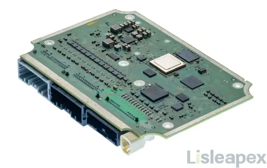
Hybrid IC Circuit Diagram
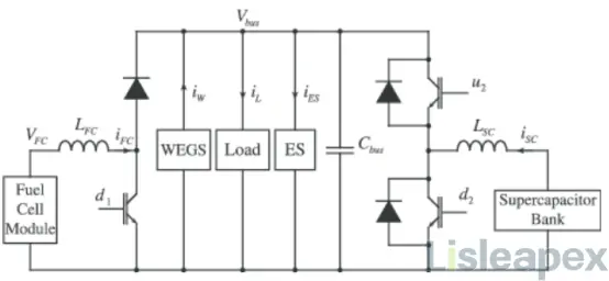
Hybrid system circuit diagram
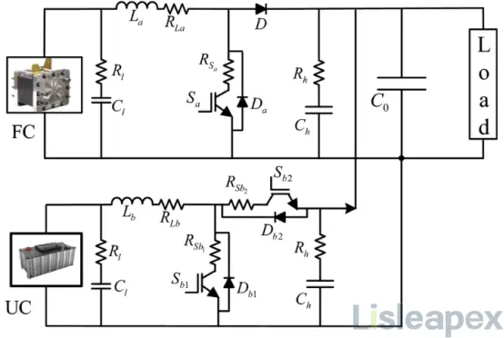
Circuit diagram of the proposed hybrid system
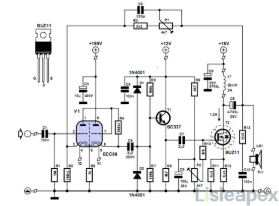
Simple Hybrid Audio Amplifier Circuit Diagram
Hybrid Integrated Circuit Fabrication Introduction
Hybrid integrated circuit (HIC) fabrication involves the assembly and integration of individual semiconductor devices and passive components onto a substrate or printed circuit board (PCB). Here's an overview of the fabrication process:
Substrate Preparation:
The fabrication process begins with the preparation of the substrate, typically made of ceramic or laminate material. The substrate provides a stable base for mounting components and forming circuit connections.
Component Assembly:
Semiconductor devices such as transistors, diodes, and monolithic ICs are separately fabricated using standard semiconductor manufacturing processes. These components are then mounted onto the substrate using wire bonding, flip-chip bonding, or other bonding techniques. Passive components such as resistors, capacitors, inductors, and transformers are also added to the substrate.
Interconnection Formation:
Interconnections between components are formed using thick film or thin film technology. In thick film technology, conductive and resistive materials are screen-printed onto the substrate and then fired at high temperatures to form conductive traces and resistive elements. Thin film technology involves depositing conductive and resistive materials onto the substrate using techniques like vacuum evaporation or sputtering, followed by photolithography to pattern the desired circuitry.
Encapsulation:
Once the components and interconnections are in place, the HIC is encapsulated to protect them from environmental factors such as moisture, dust, and mechanical stress. Encapsulation materials such as epoxy resin or plastic are applied over the entire circuit, leaving openings for external connections.
Testing and Quality Control:
After encapsulation, the HIC undergoes rigorous testing to ensure proper functionality and reliability. Various electrical tests are performed to verify circuit performance, including continuity checks, voltage measurements, and signal integrity tests. Additionally, environmental tests such as temperature cycling, humidity testing, and mechanical shock testing may be conducted to assess the HIC's durability.
Packaging and Labeling:
Once testing is complete, the HIC is packaged into its final form, which may include adding connectors, leads, or other external features. The HIC is then labeled with identification markings such as part numbers, date codes, and manufacturer logos for traceability and identification purposes.
Overall, hybrid integrated circuit fabrication involves a combination of semiconductor manufacturing techniques, interconnection technologies, encapsulation methods, and testing procedures to create compact and reliable electronic circuits suitable for a wide range of applications.
Hybrid IC Package Types
Hybrid integrated circuits (HICs) can be packaged in various ways depending on the specific requirements of the application and the type of components integrated into the circuit. Here are some common package types for hybrid ICs:
Ceramic Dual Inline Package (DIP):
Ceramic DIP packages are a popular choice for hybrid ICs due to their durability, thermal stability, and ability to accommodate multiple components on a single substrate. These packages feature leads extending from two opposite sides, making them suitable for through-hole mounting on a PCB.
Ceramic Flat Pack (CFP):
CFP packages offer a compact and flat profile, making them suitable for applications where space is limited. They consist of a ceramic substrate with leads extending from the perimeter of the package for surface-mounting onto a PCB.
Metal Can Package:
Metal can packages provide excellent shielding and protection against electromagnetic interference (EMI) and environmental factors. They are commonly used for high-reliability applications such as aerospace, military, and automotive industries.
Plastic Dual Inline Package (PDIP):
Plastic DIP packages are cost-effective and widely used for hybrid ICs that do not require high thermal performance or ruggedness. They feature leads extending from two opposite sides and are suitable for through-hole mounting.
Surface Mount Package (SMD):
Surface mount packages are designed for automated assembly onto the surface of a PCB, offering space-saving benefits and high-speed assembly. These packages come in various forms such as quad flat packages (QFP), small outline packages (SOP), and thin small outline packages (TSOP).
Chip-On-Board (COB):
In COB packaging, the hybrid IC is directly mounted onto the PCB substrate, eliminating the need for a traditional package. This approach allows for compact designs and improved thermal performance but requires specialized assembly techniques.
Custom Packages:
Depending on the specific requirements of the application, hybrid ICs may be packaged in custom-designed packages tailored to accommodate unique configurations, form factors, or environmental conditions.
Difference between Monolithic and Hybrid IC
Monolithic Integrated Circuits (ICs):
Monolithic integrated circuits are characterized by having the entire circuit constructed on a single semiconductor chip. These circuits are typically fabricated entirely on a single piece of silicon or another semiconductor material, and then enclosed in a package with connecting leads. Monolithic ICs are known for their small size, high speed, and optimized performance for specific applications. However, they offer limited flexibility in circuit design due to the constraints of the single-chip structure.
Hybrid Integrated Circuits (ICs):
Hybrid integrated circuits are fabricated by interconnecting a number of individual chips on a substrate, often made of ceramic. This substrate may carry one or more silicon chips, along with other components such as resistors, capacitors, diodes, and transistors. Hybrid circuits offer greater flexibility in circuit design compared to monolithic ICs, as they allow for the integration of diverse technologies and components. They can also adopt mixed technology, incorporating different types of chips within the same assembly.
Differences between Monolithic and Hybrid ICs:
|
Criteria |
Monolithic IC |
Hybrid IC |
|
Integration |
Entire circuit on a single semiconductor chip |
Combines multiple chips or technologies on a substrate |
|
Components |
Limited types of components on a single chip |
Diverse components (e.g., resistors, capacitors) can be integrated |
|
Customization |
Limited customization due to single-chip design |
Allows for customization with a mix of technologies and components |
|
Complexity |
Limited complexity due to single-chip structure |
Higher complexity with the integration of multiple elements |
|
Performance |
Optimized for specific applications |
Versatile and adaptable to various applications |
|
Size |
Smaller footprint due to single-chip design |
Can be larger due to the integration of multiple components |
|
Cost |
Potentially lower manufacturing costs |
Costs may vary based on the complexity and customization |
|
Reliability |
Generally high reliability for specific functions |
Reliability may depend on the integration and assembly process |
|
Applications |
Common in digital and certain analog applications |
Widely used in analog, RF, and specialized applications |
|
Technology Development |
Advances in monolithic technology continue |
Hybrid technology evolves with integration trends |
You may like: Monolithic IC vs. Hybrid IC: An In-Depth Exploration
In summary, while monolithic ICs offer optimized performance and small size for specific applications, hybrid ICs provide greater flexibility, versatility, and adaptability through the integration of multiple components and technologies on a substrate.
Conclusion
In conclusion, hybrid integrated circuits (HICs) represent a dynamic synthesis of semiconductor integration and film technology, offering unparalleled flexibility and precision in electronic circuit design. From voltage regulators to RF transceivers, HICs have permeated various industries, enabling the realization of compact, reliable, and high-performance electronic systems. Despite their challenges, such as cost and complexity, the unique capabilities of hybrid ICs continue to drive innovation and push the boundaries of electronic design. As technology evolves, so too will the role of HICs, shaping the landscape of modern electronics for years to come.
FAQ
-
What are the challenges in designing and manufacturing hybrid integrated circuits?
Designing and manufacturing hybrid integrated circuits present several challenges, including: Complexity of integration: Integrating multiple components and technologies onto a single substrate requires careful planning and coordination to ensure correct functionality and reliability. Thermal management: Managing heat dissipation in hybrid integrated circuit packaging is crucial for preventing overheating and ensuring long-term reliability. Connection reliability: Ensuring reliable connections between different components and technologies (such as wire bonds and solder joints) is essential to prevent electrical failures and performance degradation. Testing and quality control: Thorough testing and quality control measures are necessary to validate the functionality and reliability of hybrid integrated circuits, especially considering their complexity and the nature of various components.
-
Can hybrid integrated circuits be customized?
Yes, they can be customized to meet specific application requirements, allowing designers to choose components, technologies, and packaging options accordingly.
-
Are hybrid integrated circuits more expensive?
Yes, generally, due to their complex manufacturing processes and additional assembly steps, hybrid integrated circuits tend to have higher manufacturing costs compared to monolithic integrated circuits.
-
What are the differences between hybrid and monolithic integrated circuits?
Hybrid integrated circuits combine multiple semiconductor and thin-film technologies on a single substrate, often integrating discrete and active components. Monolithic integrated circuits are fabricated on a single semiconductor substrate using deposition, lithography, and etching techniques.
Stay updated with Lisleapex by signing up for the newsletter